In the late 20th century increasingly powerful and numerous personal computers and interconnected networks thereof were at the center of shifts in work practices, communications, and cultural production that collectively became known as the digital age. These personal computers were in no small part defined by two key types of electronic components: the microprocessor and the dynamic random access memory (DRAM). These components in turn were both species of silicon integrated circuits, owing both their existence and their growing power to new developments in the manufacturing technology used to create them. Computer chip manufacturers in the mid-1980s were pushing the limits of miniaturization using a variety of innovative manufacturing practices. The rise of the digital age depended on new materials and techniques that could both increase performance and drive down cost.
For decades the semiconductor industry had used photolithography to build integrated circuits on wafers cut from large single crystals of the element silicon. In the patterning process of photolithography, a polymer film called a photoresist is deposited over a thin film of one of a variety of materials deposited atop a silicon wafer. Next, in a complex (and expensive) apparatus known as an exposure tool, light of a very specific wavelength is projected through a pattern-bearing mask onto the photoresist. Regions of the photoresist exposed to the light undergo chemical changes, making them either more or less susceptible (depending on the process) to being removed in a subsequent chemical developing process. Thus the pattern of the mask is transferred to the photoresist. The pattern from the photoresist is then transferred to the underlying thin film through a subsequent process of chemical etching. Multiple iterations of this thin-film patterning process, along with several other physical processes, produce integrated circuits. The photoresist is at the center of the photolithographic process, just as film used to be the crux of photography.
In the late 1970s photolithographic procedures used light from the near-ultraviolet (UV) and mid-UV ranges at 365 and 313 nanometers (nm), respectively. Manufacturers realized that moving to a shorter wavelength, the so-called deep UV, at 248 nm or less, would allow even smaller patterning of integrated circuits, thereby continuing the dynamics of miniaturization, exponential increases in functionality, and dramatic decreases in cost that characterize Moore’s law. Making the leap to deep UV would require dramatic materials innovations and a sea change in photoresist technology. An entirely new breed of photoresist—chemically amplified (CA) photoresists—created within IBM in the early 1980s for just this purpose would eventually come to dominate global semiconductor manufacture. More recently, a later generation of chemically amplified photoresists tuned to 193-nm light has continued to enable Moore’s law. For nearly two decades CA photoresists have stood behind the digital age, largely unrecognized and undeservedly so.
Pushing the Limits at IBM
Some commentators describe the digital computing business in the late 1970s as divided into halves, with IBM on one side and all the other companies on the other. Despite thriving competitors in the minicomputer business and the appearance of the very first personal computers, IBM dominated the computer industry with its broad offering of mainframe and mid-range computer systems, largely produced by captive suppliers within IBM. Large semiconductor fabrication operations in East Fishkill, New York, and Burlington, Vermont (among other locations), produced integrated circuits as logic and memory components. Many of the materials for these semiconductor fabrication plants, or “fabs,” came from additional operations in East Fishkill. In San Jose, California, a disk-drive manufacturing facility boasted a research laboratory. On the East Coast, Yorktown Heights, New York, was the site for the firm’s research and development headquarters.
Throughout the 1970s IBM produced its own photolithography equipment. As the decade drew to a close, however, IBM began to purchase significant numbers of sophisticated and expensive optical devices from the outside, particularly the Micralign lithography tools produced by the venerable optics house and chemical-instrumentation manufacturer PerkinElmer. IBM’s production facilities for advanced semiconductor components contained hosts of self- and PerkinElmer– produced lithography “tools.” These capital goods represented an enormous expenditure, with each tool having cost hundreds of thousands of dollars. In the same period, the fate and future utility of these existing tools were being seriously questioned within IBM.
By the time the 16K DRAM generation was launched in 1977, semiconductor memory was well on its way to displacing magnetic core memory as the dominant memory technology for digital computers. DRAMs were considered the shining examples of so-called large-scale and even very-large-scale integrated circuits in which huge numbers of components were squeezed onto tiny chips of silicon using the latest manufacturing technology, yielding expanded memory functionality at declining costs. Magnetic core memory, in contrast, hailed from the 1950s and consisted of great grid-like planes of wires with small metal rings at each intersection: think of the screen in a window, with a miniature washer around the corner of each little square. The magnetic states of these rings, or “cores,” represented the digital language of zeros and ones. First introduced in 1970, DRAMs were beating out cores on both performance and cost just six years later.
The success of DRAM depended on the semiconductor industry’s ability to push its manufacturing technology to the limits. Indeed, DRAM production became the bellwether for such technology. The semiconductor industry, led by Intel, had established a metronomic pattern in which the industry launched a new generation of DRAM with four times the capacity of the previous generation—1K, 4K, 16K—every three years. Each generation required a new level of miniaturization, thereby creating a fundamental link between DRAM generations and manufacturing technology.
In 1977 a looming question for the semiconductor industry was whether or not the existing lithography tools for the 16K DRAM generation could be used again for the upcoming 64K DRAM generation or perhaps even for the 256K DRAM generation. The ability to form smaller features depended on the wavelength of light used in the tool: the smaller the wavelength, the smaller the possible features. The existing lithography tools used 365 nm light in the near-UV region to expose patterns onto silicon wafers coated with photoresists. Could the existing lithography tools and photoresists be modified to work with smaller wavelengths of light? The economic consequence of the answer was significant. Millions of dollars could be saved if the useful life of the manufacturing equipment could be extended.
Pausing at 313
Extending the life of IBM’s lithography tools and photoresists was a major challenge that C. Grant Willson absorbed when he joined a research group focused on polymer science and technology at IBM’s San Jose operations. Willson, a Bay Area native, had earned his PhD in organic chemistry at the University of California, Berkeley, and had been working at the University of California, San Diego, doing research in biochemistry. Although it was generally recognized in the semiconductor community that significantly lower wavelengths would eventually be needed to get the required miniaturization, the San Jose polymers group was exploring the extension of near-UV lithography for upcoming DRAM generations. The IBM researchers saw an opportunity to extend the usefulness of their tools by moving to an “intermediate wavelength,” a halfway point between the current near-UV and the future deep UV.
The attraction of this intermediate step was savings: they could postpone the need to refit factories with the new tools and resists that they knew would eventually be required for the deep-UV regime. Moreover, this intermediate wavelength step—to 313 nm from 365 nm— would buy the researchers time to tackle the more radical developments that would be necessary for the eventual migration to the deep UV. Willson’s first great success in photoresists was to develop a modified version of the standard type of near-UV photoresist, known as the DNQ-Novolac resist, but tuned to work with 313-nm light and to be compatible with existing lithography equipment. Willson’s proprietary resist was used for both 313-nm and traditional near-UV lithography and in a few short years suffused IBM semiconductor manufacturing. The resist gave IBM a competitive advantage in the form of tremendous cost savings by extending the utility of IBM’s existing tools and device performance advantages through successful miniaturization. Willson had established himself as a leader in photoresists within IBM.
By 1979 Willson was focusing on a more challenging prospect: the move to deep UV. By this time IBM was anticipating the delivery of new PerkinElmer lithography tools to its fabs—the PerkinElmer Micralign 500. This tool used a mercury lamp that generated UV radiation with intensity peaks at 365, 313, and 248 nm. The use of an appropriate filter made the tool capable of operating at any one of these wavelengths. The 248-nm wavelength was in the deep UV region, but at that wavelength the lamp emitted only 1/30 the amount of light as it did in the other UV regions. This relative dimness raised serious challenges.
Existing photoresists did not have enough sensitivity for working with such a low intensity. A work-around was possible with unprecedentedly long exposure times, but that was an economic nonstarter. Grindingly slow fabs would destroy any savings from extending the tools. The IBM researchers had two remaining options: create a new lamp for the tools that was 30 times brighter at 248 nm, or invent a photoresist that was 30 times more sensitive to 248-nm light than the DNQ-Novolac resists.
A Chemical Solution
Willson focused on the chemical challenge: could he create a new photoresist with 30 times the sensitivity? Willson discussed this situation with a visiting scientist who joined his group in the first days of 1979: Jean Fréchet. Fréchet, born in France, was an accomplished polymer chemist on sabbatical at IBM in San Jose from the University of Ottawa. In discussions between Willson and Fréchet the essence of the needed innovation emerged: chain reactions. They imagined a photoresist in which a single photochemical event—the absorption of a photon by a material in the resist—could generate a cascading chain reaction. The chemistry of the photo-resist would amplify the effect of the photochemical event, yielding the great sensitivity that was their goal.
Fréchet quickly advanced a particular polymer as a possible candidate for use in such a system: polyphthalaldehyde (PPHA). This polymer chain is unstable at room temperature; its propensity is to unzip, to depolymerize. The only way to stabilize the polymer at temperatures up to 200°C is to cap the chain with a chemical group. Both the polymer chain and the capping groups are highly susceptible to cleavage by acid as well. Fréchet and Willson considered the possibility that irradiation could directly break bonds in the back bone of the polymer, causing the PPHA to depolymerize. Once started, the polymer would unzip in a chain reaction.
Fréchet synthesized PPHA samples so that he and Willson could begin to work with it. By the summer of 1979, however, it became clear to Fréchet that the project could not be completed before his sabbatical ended. At Fréchet’s urging Willson made a recruiting trip to the chemistry department at the State University of New York’s College of Environmental Science and Forestry in Syracuse, where Fréchet had earned his Ph.D. There Willson met Hiroshi Ito, a research associate in the department with a Ph.D. in polymer chemistry from the University of Tokyo. Ito, like Fréchet, had experience with the special techniques required to synthesize PPHA. Willson offered Ito a postdoctoral position in his San Jose group, and in the summer of 1980 Ito joined the lab.
Ito took over where Fréchet left off, beginning by synthesizing PPHA by new means to produce a more temperature-stable polymer. Ito irradiated his PPHA, and the result was more a fizzle than a chain reaction: there was depolymerization, but not enough. Ito’s next move was to mix a well-known photoacid generator (PAG) into his PPHA and expose the mix to deep-UV light. PAGs are compounds that generate acid when exposed to light. Since both the PPHA chain and its capping group could be cleaved by acid, Ito thought the PAG might initiate the desired chain reaction. This time half of the PPHA unzipped. This was far better but still not good enough.
Meanwhile a new class of PAGs based on onium-salt compounds had recently emerged from both 3M and General Electric. These onium-salt PAGs produced notably strong acid, and many had the added virtue of stability at high temperatures. The potential of these new PAGs for polymer chemistry was broad, and the PAGs quickly generated interest. Remarkably, Willson learned about the 3M PAGs at almost the same time that Ito alighted upon the General Electric PAGs. Ito had been searching for another PAG to add to PPHA—one that was more temperature-stable and produced stronger acid than the traditional PAGs. At General Electric the chemist James Crivello had invented triphenylsulfonium hexafluoroantimonate (TPSHFA) for UV-induced polymerization, or “curing,” of epoxy resins. This onium salt generated a strong acid that catalyzed the polymerization. Ito hoped that in his PPHA photoresist system, the onium-salt PAG would initiate a strong chain reaction of unzipping.
Willson vividly recalls the day when Ito first tested his novel mixture of PPHA and Crivello’s PAG as a deep UV photoresist. The results, Willson recalls, were “remarkable.” With the new onium-salt PAG and a dose of UV light 100 times less intense than that used in conventional photolithography, the PPHA rapidly and fully unzipped. Not only did the materials unzip, but the exposed regions of Ito’s mixture also completely vaporized, laying bare the underlying substrate. Ito’s material was a dramatic proof of concept of the chemical amplification scheme that Willson and Fréchet had advanced the previous year. At hand was a material with high resolution (the ability to produce fine patterns), high speed, and tremendously improved sensitivity to deep-UV radiation. Yet Ito’s PPHA system worked too well and not well at all. The vaporized photoresist material would hopelessly contaminate the lithography tools. Further, PPHA’s susceptibility to acid meant that it could offer little protection from acidic etching procedures and hence would be of little to no use in actual device fabrication.
Ito’s material was a dramatic proof of concept of the chemical amplification scheme that Willson and Fréchet had advanced the previous year.
Willson and Ito turned to another polymer that Fréchet had worked on earlier at IBM San Jose during his sabbatical there in 1979: poly(p-hydroxystyrene), or PHOST. PHOST is a styrene-based polymer, chemically similar to the Novolac resins used in conventional photoresists. Willson suggested modifying the polymer to include a new side chain: tertiary butoxycarbonyl, or tBOC. The resulting polymer was poly(p-t-butyloxycarbonyloxystyrene), or PBOCST. Willson, who had worked mainly in biochemistry before joining IBM, was aware that tBOC—a mainstay in peptide work—was susceptible to cleavage from the basic polymer through the action of both heat and acid. Willson and Fréchet recall early, inconclusive attempts by Willson and several coworkers to make a PBOCST resist based on acid-catalyzed cleavage of the tBOC groups using photosensitive orthonitrobenzyl esters to produce the acid. From Ito’s perspective the PBOCST work was dormant when he reached the lab. However, Ito also began investigations of photoacid-catalyzed cleavage of a different tBOCprotected polymer as a potential basis for a chemically amplified resist. Looking at Ito’s results, Willson and Ito decided to pursue a hybrid course: mixing PBOCST with the onium-salt PAG. The result of this mixture—the brew resulting from the experiences and interests of Fréchet, Willson, and Ito—stopped the researchers in their tracks.
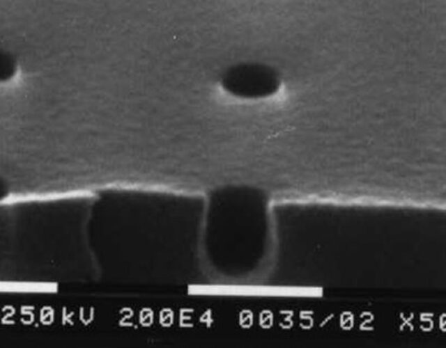
The tBOC resist displayed dramatic chemical amplification. After exposing the tBOC resist to 248-nm deep-UV light, the resist-coated silicon wafer was heated in a post-exposure bake. The acid generated by the onium salt catalyzed the cleavage of the tBOC groups. The resulting fragments then generated additional acid, catalyzing further tBOC cleavages in a cascade of de-protection. The reaction was both extremely fast and extraordinarily sensitive to the deep-UV light. At the beginning of his search for a CA resist Willson knew that he needed a 30-fold improvement in sensitivity over conventional resists. With the tBOC resist, Willson, Fréchet, and Ito had generated a 100- to 200-fold improvement.
By 1983 Willson was confident enough in the new tBOC resist to promote it within IBM. At East Fishkill he presented it to a collection of researchers and engineers from a variety of IBM sites, including representatives from East Fishkill’s own photoresist operation and staff from the cutting-edge fab in Burlington. John Maltabes, a lithography engineer from the Burlington plant, had been helping develop a manufacturing process for a 1M DRAM using deep-UV radiation to meet a “1 micron design rule.” Deep-UV lithography would be used to produce features as small as 1 micron on the new powerful memory chip. Maltabes had been evaluating the possibility of replacing the mercury lamps within the PerkinElmer lithography tools in Burlington with excimer lasers. But Willson’s tBOC presentation persuaded Maltabes that using the new photoresist with the existing mercury lamps was the better strategy: when he returned to Burlington, Maltabes tried to convince his supervisors to kill his project. Three months later they did just that. Maltabes’s new job would be to help implement the tBOC resist for manufacturing the 1M DRAM.
Something in the Air?
IBM had staked the future of its cutting-edge products on CA photoresists. The advantages were tremendous: the tBOC resist could save IBM millions of dollars in modification and replacement of its existing lithography tools. The downside was the uncertainty that the new resists would work in an active manufacturing environment.
Production trials at Burlington, however, revealed new, unanticipated problems with the CA resist. For one, its sensitivity varied widely. After eliminating the lithography tools as the source of this unpredictability by installing new, exacting filters, the blame rested squarely on the tBOC resist. Eventually, the production engineers in Vermont resorted to the kind of highly empirical “black magic” practices that characterized much of semiconductor manufacturing in its early years. They did not know why certain things worked, only that they did. The engineers found, for instance, that letting silicon wafers that had been coated with the tBOC resist sit for several hours in the factory before exposing them stabilized the sensitivity, but at a lower level.
More troubling was the occasional formation of “skins” in the uppermost layer of the tBOC resist. These skins were regions of the photoresist in which sensitivity had catastrophically collapsed. Exposed regions of the resist near the surface would not develop properly and thus formed a skin that could not be removed by the solvent. Puzzlingly, these skins were all at the surface of the resist. Regions of the resist directly below these skins developed perfectly. The issue was serious: these skins would result in fatally defective DRAMs.
IBM had staked the future of its cutting-edge products on CA photoresists.
The groups at San Jose, Burlington, and East Fishkill were troubled by the new resist’s difficulties. Maltabes recalls a lunch conversation in San Jose about these issues in which a researcher who had experience manufacturing disk-drive systems suggested that these troubles stemmed from “something in the air.” This researcher and his colleagues had attributed certain failures of disk-drive systems to airborne contaminants and had used air-filtration systems with activated charcoal and HEPA filters to get around the problem. Surplus filtration units sat in a warehouse, and he offered them to the tBOC team.
Maltabes and Scott McDonald from Willson’s team returned to Burlington with the surplus units. With a series of experiments the pair determined that in filtered-air environments, and indeed environments of air pumped in from outside the fab, the skins disappeared and the resist sensitivity was both high and consistent. The atmosphere of the fab itself harbored contaminants that were responsible for the problems with the tBOC resist. With pressure mounting to get the 1M DRAM into full production, Burlington decided to filter the air rather than hunt down the unknown contaminant or contaminants. Once wafers were coated with the tBOC resist, they remained in a filtered-air environment until they entered the lithography tool.
By 1986 1M DRAM production was in full swing. IBM manufactured several million of these DRAMs, all dependent on the CA tBOC resist. Reflecting the criticality of tBOC resists to the success of this project in moving IBM to the first deep-UV manufacturing technology, the firm kept the tBOC resist as a proprietary material and the use of filtered air as a closely held trade secret into the early 1990s. Several million working DRAMs within IBM’s flagship computer products offered powerful testimony: the era of CA photoresists had arrived.
Coda
For IBM, possession of the first CA photoresist conferred significant competitive advantage. By the mid-1990s, however, a combination of accidental and systematic factors broke IBM’s exclusive hold on this class of material. Willson, Fréchet, and Ito had patented the tBOC resist in 1982, but the patent was limited to just the tBOC material, not the very idea of a CA photoresist. This limited scope was the product of multiple factors: the large role played by the researchers rather than attorneys in writing the patent; the vagaries of process patenting in comparison with patents on particular materials; and the discovery of “prior art” in the patenting process. One of the developers of onium-salt photoacid generators at 3M, George Smith, had previously patented a photoresist involving a very similar mechanism to the tBOC resist. These accidental factors allowed commercial photoresist producers—inspired by IBM’s success— to bring their own versions of CA deep-UV resists to the market by the early 1990s.
More systematically, CA photoresists escaped IBM as the computer giant participated in the growing trend among semiconductor manufacturers to obtain manufacturing equipment and materials from specialized external suppliers. As IBM came to rely more heavily on lithography tools produced by outsiders, the close coupling of tool with resist meant not only that the tool makers would need access to the best CA resists but that the tool makers’ other customers would also require access. Moreover, specialized photoresist houses had greater resources and incentives for pushing CA photoresists forward. In the mid-1990s IBM actively transferred the second- and third-generation CA photoresists developed by Ito and others to the outside world. In doing so, IBM accelerated future developments in CA resists, empowering the continued evolution of the digital age.
The author wishes to thank CHF’s Gore Innovation Project for the support of the research leading to this article; Hiroshi Ito, C. Grant Willson, John Maltabes, and William Brunsvold for their time and candor in a series of research interviews; and Christophe Lécuyer for his revealing oral history with Jean Fréchet.